# Mega Tutorial - ETL Test Stand
The ETL Test Stand is a setup at various sites to test the various components that will ultamitely make up the particle detector. The aim of this tutorial is to explain how all these components work together.
## In Depth Overview
First, it is important to familiarize ourselves with the each of the players that make up the ETL Test Stand and how they work.
### Sensor Module
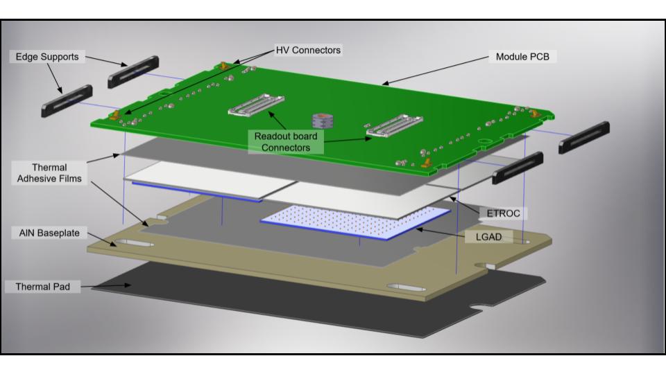
The Sensor Module and the parts inside is how we obtain the timing data for the particles. Here are the core components of an ETL Sensor Module and an overview of the basic idea behind them.
#### ETROC + LGAD Subassembly
There are four square (Endcap Timing ReadOut Chip + Low Gain Avalanche Diode) ETROC+LGAD Subassemblies on a module. Each LGAD and ETROC is a 16x16 array of pixels and a pixel is about 1.3x1.3 mm^2^.
| Bump Bond | Picture |
| -------- | -------- |
| Each pixel on the LGAD is bump bonded (a bead of metal to provide electrical connection) to a corresponding pixel on the ETROC. This is how the signal moves from the LGAD to the ETROC. | <img src=https://codimd.web.cern.ch/uploads/upload_cca5cb2b0e56316876c09cc5df47b033.png width="1000"/>|
##### THE LGAD

> Figure from Reference 1
The basic idea of the LGAD is that each pixel is like a reversed bias PN junction (there are a lot of good resources on the [PN junction](https://youtu.be/JRf2VuwBVvs?si=FQ2Wk2AtNBpUMUho)). If a charged particle rams into the depletion region it can free up some charge carriers that get collected on the terminals. This is *the signal* that gets passed to the ETROC pixel. This also gives intuition about how charged particles with different energy cause larger or smaller signals.
* [A paper about the LGAD I wrote](https://docs.google.com/document/d/1bf8d8TjICwP8_iA7hSKjkzaHNtp3uApHB-sH30cLk6E/edit?usp=sharing)
* [Wait how do we think about Voltage again?](https://electronics.stackexchange.com/questions/245610/is-voltage-the-speed-of-electrons)
##### THE ETROC
The main purpose of the ETROC is to digitize the analog signal and calculate the desired timing information that will be read out (hence the name Endcap Timing ReadOut Chip). Now we will go over how the signal is processed in the ETROC and timing information is obtained.
###### 1. Signal Amplification
The signal from the LGAD is passed through a [preamplifier](https://en.wikipedia.org/wiki/Preamplifier). The preamplifier converts a weaker electrical signal into a stronger one for further processing, minimizing disruption from noise.
###### 2. Signal Discrimination
The amplified analog signal pulse is converted into a digital pulse by a [discriminator](https://docs.nscl.msu.edu/daq/samples/Discriminators.pdf).
| Discriminator | Picture |
| -------- | -------- |
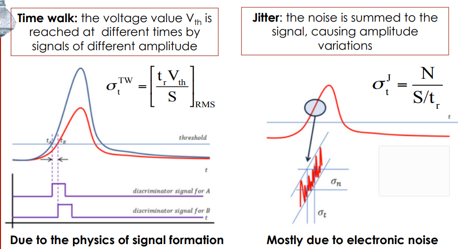
| Discriminators are often used in data acquisition electronics setups. They decide when the input signal is of interest by putting out a logic pulse when the input signal meets an adjustable threshold value. Discriminators fall into two categories: **leading edge** and **constant fraction**. A **leading edge discriminator** looks at the leading edge of the signal and emits a logic pulse when the signal reaches the threshold level. However, this can lead to "walk," which is a timing variance depending on the size of the signal. | <img src=https://codimd.web.cern.ch/uploads/upload_924575a54af7eb4a00443bfd238dd964.png alt="drawing" width="5000"/> |
The threshold voltage of the ETROC is very important because it determines when we want to count a particle hit.
###### 3. Timing Measurement
The signal is then passed to a low power Time-to-Digital Converter ([TDC](https://en.wikipedia.org/wiki/Time-to-digital_converter)). The TDC measures calculates two pieces of timing information: the **Time Of Arrival (TOA)** and the **Time Over Threshold (TOT)** of the signal that was generated from the particle passing through a pixel on the LGAD. See [here](#Getting-Timing-Information) about TOA and TOT. It knows when the particles first collided because an input to they system is the frequency of collisions at the HL-LHC (40MHz).
The timing information is stored in a [circular buffer](https://en.wikipedia.org/wiki/Circular_buffer) in each of the pixels of the ETROC. Thevcircular buffer uses First In First Out (FIFO) logic for the data. Data is only ever read out by recieving a Level One Acceptance signal (L1A, more on that later).
* [ETROC2 Manual](https://indico.cern.ch/event/1288660/contributions/5415154/attachments/2651263/4590830/ETROC2_Reference_Manual%200.41.pdf)
* [Paper about how ETROC works, TOT, timewalk, CFD vs Leading edge discrimnator](https://arxiv.org/pdf/2012.14526)
#### Module PCB
<img src=https://codimd.web.cern.ch/uploads/upload_e70a990eee8cc18cbe90ce4512072984.png width=50% style="display: block; margin: auto">
The Module PCB houses the 4 ETROC+LGAD sensors and passes the signal along to the next layer (The Readout Board) via board to board connectors on the back. Each ETROC+LGAD subassembly has a bunch of tiny wires connecting the ETROC readout to the Module PCB (we call them wirebonds).
> Needs more of an explanation of the propogation of signal and what it tries to do til it is at the board to board connectors
### The Readout Board
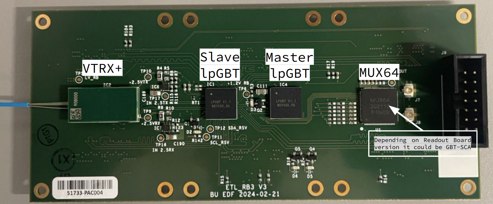
The Readout Board allows for 3 Sensor Modules to be connected to it via board to board connectors. The Module PCB that holds the 4 LGAD+ETROC subassembly connects to it. The Readout Board handles the connection between the modules and the backend data acquisition (DAQ) of ETL. That communication is done through [optical fibers](https://en.wikipedia.org/wiki/Optical_module) (optical fibers let you transmit a lot of data quickly). The optical transciever that connects the Readout Board and the KCU is called the VTRX+.
#### lpGBTs
* https://cds.cern.ch/record/2809058/files/lpGBT_manual.pdf
> The Low Power Giga Bit Transceiver is a radiation tolerant ASIC that can be used to implement multipurpose high speed bidrectional **optical links** for high energy physics experminets --The Manual
* **Electrical links (eLinks)** = these connect the lpGBT with the ETROC. See section 1.2.2 of the manual.
* **Downlink** = data in the direcion from the DAQ (KCU) to the detectors (Module/subassembly)
* **Uplink** = data in the direction from detectors to the DAQ
TEMP
* https://etl-rb.docs.cern.ch/files/etl_rb3_mux64.pdf
* https://twiki.cern.ch/twiki/pub/CMS/ModulePCB/ETL_FE_electronics_April2024.pdf
##### DAQ LpGBT (MASTER)
Sends 320MHz clock to ETROC (through the module)
Handles I2C to ETROC (through the module)
Sends data to VTRX+
##### Trigger lpGBT (SLAVE)
Sends data to VTRX+
#### The ADC - MUX / GBT-SCA
#### VTRX+
Mostly the VTRX converts the signal between optics and copper. It is somewhat "smart", you can control drive strength of the laser (just makes the laser brighter) and can read the VTRXs temperature. It was also designed to work between the lpGBTs and an FPGA (KCU).
Data can obviously flow between the KCU and lpGBT and vice versa (bi-directional). It has 4 up-stream (frontend to backend, lpGBT to KCU) channels (10.24 Gb/s) and two down-stream (backend to frontend) channels (2.56 GB/s).
* https://edms.cern.ch/ui/file/2149674/1/VTRxPlusApplicationNote.pdf
### KCU (the backend DAQ)
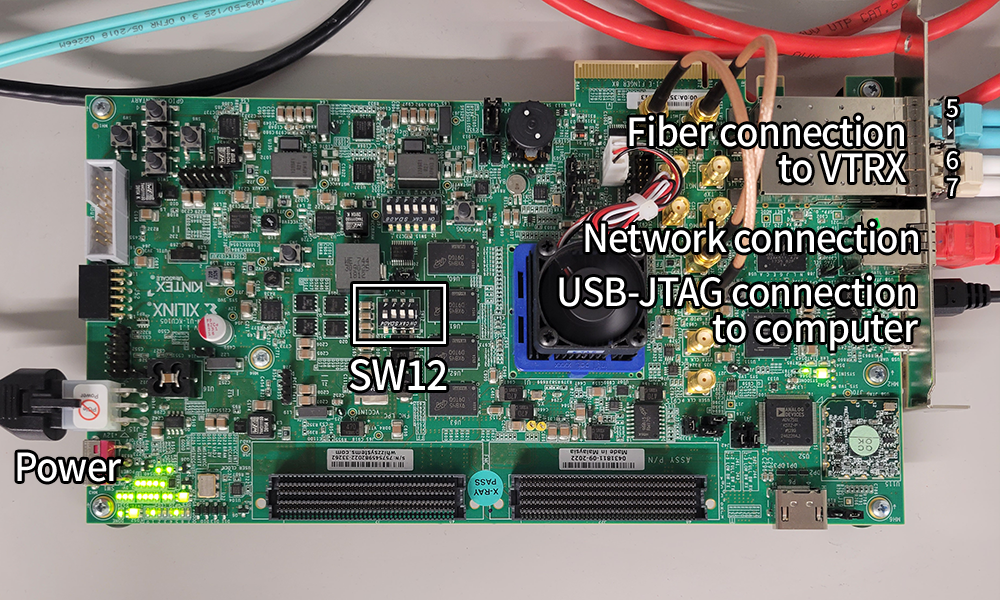
The KCU is a [FPGA](https://en.wikipedia.org/wiki/Field-programmable_gate_array), it can request data to be read out from the Readout Board through the VTRX connection.
Backend board (KCU 105): Communicates with the frontend (readout board, ETROC) through optical high speed links (2 uplinks RB->KCU, 1 downlink KCU->RB). Controlled from a PC through local network using IPBus library within the tamalero software package. Provides the LHC clock to the frontend and ETROC.
| Power | SW12 | USB-JTAG | Network Connection | Optical Fiber |
| ------------------------------------------------------------------------------------ | ---------------------------------------------------------------------------------------------------------------------------------------------------------------------------- | ------------------------------------------------------------------- | ------------------------------------------------------------------------------------------------------------------------------------------------------------------- | ------------------------------------------------------------------------------------------------ |
| This just powers the KCU, and teh Power label rests right on top of the power switch | SW12 lets you choose the KCU IP address. Here is how it works. See the bottom of this from the [RB docs](https://etl-rb.docs.cern.ch/Hardware/#kcu105-network-configuration) | This lets you set the firmware for the KCU, whole point of an FPGA! | This is ethernet cable that provides communiction between the KCU and the Test Stand computer. In order for it to be used the IPbus software needs to be installed. | This is how the communication between the ReadoutBoard (and subsequently the rest of the system) is done through these fiberoptic cables |
#### KCU Set Up
In order for the software on the PC to communicate with the KCU, three things need to happen. I am following the outline from this [sop from ian reed](https://github.com/nebraska-silicon-lab/Lab-Instructions/blob/master/sop/ETL/200%20-%20ETL%20Test%20Stand%20Setup.md). Steps two and three require a piece of software called [Vivado](https://en.wikipedia.org/wiki/Vivado). It is used to program FPGAs which is what the KCU is!
1. IPbus software is required
- The IPbus allows information from the KCU to be communicated over an IP address. The IP address is used by the computer and hence the software to communicate to the KCU.
- [CERN IPbus docs](https://ipbus.web.cern.ch/doc/user/html/index.html).
- And, for a rough conceptual understanding see the [Brief Introduction to IPbus](https://ipbus.web.cern.ch/introduction)
2. The Clock of the KCU needs to be set
- ??? What does the clock do for the KCU and how is it needed for the rest of the test stand
- 320MHz Clock
- 8 times 40MHz clock. 40MHz is the bunch crossing frequency of the LHC (Not exactly 40MHz). This is how we know when the particles collide in the LHC by having collisions at this frequency. So we need to tune our equipment to this to get any timing information
3. The firmware needs to be loaded
- The firmware does ???
- See this https://etl-rb.docs.cern.ch/Firmware/rb-firmware/ or sop from ian reed above
- https://en.wikipedia.org/wiki/Firmware
- The firmware is installed through the USB-JTAG on the KCU, if you download the firmware it is ran with `program.sh` script in the installed firmware directory. (Put yes on the first prompt and no on the second!)
#### Setting Up KCU For Software
- Once the IPbus software is on the computer it does not need to be worried about again. And can be activated by running:
- `/opt/cactus/bin/controlhub_start`
- Through Vivado the clock on the KCU should never change even through reset. It was configured this way
- To check if the clock was configured right, type `screen /dev/ttyUSB<usb port number> 115200` if usb port number is 1, itd be `/dev/ttyUSB1`. Then it should be blank, hit enter and a menu should appear. Then just type the number and you can navigate, do (1) -> (7) to read if the clock is 320MHz. For more info: https://etl-rb.docs.cern.ch/Hardware/#configuring-a-new-kcu-105-eval-board
- The firmware will need to be reloaded at times and you go to the firmware directory that looks something like `etl_test_fw-v2.1.11` and within the directory run `source program.sh` (for the first prompt put yes and the second put no). That second prompt is about loading the firmware persistantly and that does not currently work but is not needed
- You might need to put vivado in path: `source /tools/Xilinx/Vivado_Lab/2021.1/settings64.sh`
#### Resources
* https://gitlab.cern.ch/cms-etl-electronics/module_test_fw/
## Data Acquisition
### S
## Data Flow
## Software
Remember to set the correct paths with `source setup.sh`
### Address Tables
Do what? vs the Configurations...
### Configurations
> Need to explain in a broader sense what they do, give tutorial to updating one, addresses, how they are layed out etc...
There are different configurations for all the pieces of the Test Stand. To be verbose here is a list of all things that need to be configured (it will obviously depend on the versions or each too):. On the ReadoutBoard: GBT-SCA or MUX64, and lpGBT and the module has a config.
Depending on the version of the readoutboard need mappings for the SCA
* [configs/SCA_mapping.yaml](https://gitlab.cern.ch/cms-etl-electronics/module_test_sw/-/blob/master/configs/SCA_mapping.yaml) or [configs/SCA_mapping_v2.yaml](https://gitlab.cern.ch/cms-etl-electronics/module_test_sw/-/blob/master/configs/SCA_mapping_v2.yaml)
## Test Stand Operational Notes
### Power Cycling KCU
When you power cycle the KCU you have to turn off a switch next to the power input. It is also next to all the green lights. From the picture in the Overview section of this document, the power switch rests right on top of the `Power` label in the image.
Then you will have to reinstall the firmware and start the IPbus. See KCU set up from the Overview!
### Power Cycling RB and Modules
You can actually do this through the command line in tamalero. All that is needed is a correct power supply (`SIGLENT SPD3303X-E Programmable DC Power Supply`) and an ethernet connection to the PC.
To power down:
`python3 power_cycle.py --ip 192.168.0.25 --power_down`
To power up/cycle:
`python3 power_cycle.py --ip 192.168.0.25 --verbose`
### Learning
From the [gitlab repository](https://gitlab.cern.ch/cms-etl-electronics/module_test_sw), you can find a tutorial in the [readme](https://gitlab.cern.ch/cms-etl-electronics/module_test_sw#with-a-physical-readout-board) to connect to the KCU and ReadoutBoard manually.
### Common Commands for Operation
##### Powering up the readout board
`python test_tamalero.py --power_up --kcu <KCU address> --configuration "modulev1"`
##### To check the communication between the lpGBT and the ETROCs
`ipython3 -i test_tamalero.py -- --kcu 192.168.10 --verbose --configuration modulev1`
Then, do this line once it puts you into interactive mode:
`rb.DAQ_LPGBT.I2C_read(0x0, master=1, slave_addr=0x60)`
Where the `0x0` is the address to the module, and `0x60 `is to an ETROC! This should return a number I think. The address for each ETROC are defined in the `modulev1_v2.yaml` file. This will potentially enlighten what each of those things mean. Also `0x0` is the module position on the RB.
#### More, but more likely to change over time:
Threshold scan,
`python3 test_module.py --configuration modulev1 --moduleid 103 --test_chip --threshold auto`
Qinj,
`python3 test_module.py --configuration modulev1 --moduleid 103 --test_chip --threshold auto --qinj`
## Questions
* Does ETROC make its own clock? Or is it provided externally (by KCU?)?
* ETROC does not make its own clock but it does come from KCU
* Explain 320MHz clock vs 40 MHz clock, why doe we need LHC clock and what does it correspond to exactly?
* Both are multiples of the LHC bunch crossing clock, this is how we get the timing info, since 40MHz tells us when particles collide we just need to calculate the time from this hit, or clock rising edge
* How does the TDC work? -> how does it get TOA and TOT
* Where does the t=0 start for the TOA and how is it made useful?
* It should start at the rising or falling edge of the 40MHz clock (manual says falling edge?)
* what does it mean to write to an address location when everything is seperated
* Naomi: It is a bug if there is a shared address between the different pieces of hardware. So everything has a unique address even across hardware.
* From briefly reading the manual it seems like the lpGBT has to be configured in a c ertain way for rad hardness. Is this true and has it been done? For example:
* > Strictly speaking, the user is not required to have access to I2C nor IC/EC interfaces. However, in areas with high
radiation levels where the e-fuses can fail (see Section 3.8) it is recommended to foresee a way to communicate with
the lpGBT to check if the initialization process was successful. In case problems are detected the lpGBT should load
configuration from ROM and the remaining configuration should be provided via one of the configuration interfaces. --page 28 of lpGBT manual
* How do you find the addresses for the ADCs
* A manual/data sheet?
* In the etroc manual they have the 40Mhz clock rise edge in front of the pulse, isn't that the wrong Time of Arrival?
* what are the address tables for in the tamalero software?
* what does it mean to properly reset the system between scripts, give examples and conceptual meaning.
## Resources
[ 1 ] [4D Tracking with silicon detectors](https://iopscience.iop.org/article/10.1088/1361-6633/aa94d3/pdf?casa_token=n-oW8ROm1IMAAAAA:6KfnRwtEqIIbo5orYfdgG3GfgH4wfyDxuIDtnHbxFF_jZygOH1MjGyj9eYw_d0-oe1upJ5Ho1BCtpdzahDKtEyrE_A)
[ 2 ] https://twiki.cern.ch/twiki/pub/CMS/ModulePCB/ETL_FE_electronics_April2024.pdf
----
# BACKGROUND INFO / EXTRA
## Getting Timing Information
> How a TDC works: https://en.wikipedia.org/wiki/Time-to-digital_converter
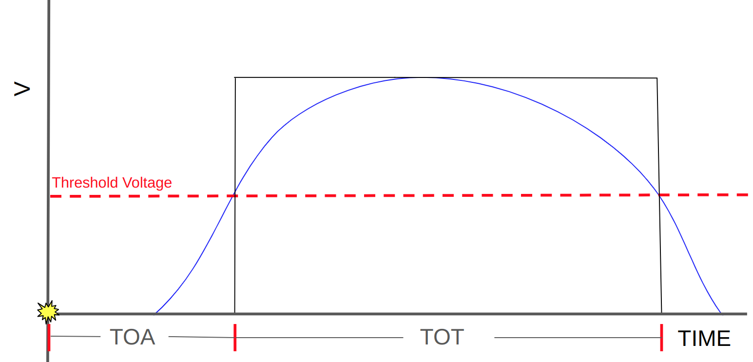
The TDC of ETROC gets this information and stores it in the circular buffer. It knows when the particles initially collided (the inputted 40MHz beat frequency of the LHC to the ETROC) and when they hit the sensor (passed the threshold voltage). So it then can calculate the following.
Time Of Arrival (TOA) is the time it takes for the signal to reach the detector and cross the threshold potential V~th~.
Time Over Threshold (TOT) is the amount of the the signal is above the threshold voltage.
| TOA and TOT Graphic, t=0 is defined as the rising edge of the 40MHz Clock or the particle collision! |
| -------- |
|  |
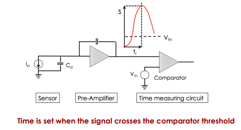
* https://indico.physics.lbl.gov/event/182/attachments/299/320/UFSD_Cartiglia.pdf
### How does the TDC get the TOA and TOT info in the ETROC?
| **Signal** | **Description** |
|-------------|-----------------|
| CLK40M | The 40 MHz TDC clock, in sync with the 40 MHz readout clock. |
| CLK320M | The TDC reference strobe which are two pulses derived from a 320 MHz clock. |
| PULSE | The TDC input or the discriminator output. **SO THE SIGNAL from the particle** |
| START | A TDC internal signal used to control the GRO, related to PULSE and the reference strobe (CLK320M). |
| TOACLK | A TDC internal signal used to latch the GRO status for TOA measurement, related to the first rising edge of the reference strobe (CLK320M). |
| TOALATCH | A TDC internal signal used to latch the GRO status that is previously latched with TOACLK, related to TOACLK. See reference [3] for details. |
| TOTCLK | A TDC internal signal used to latch the GRO status for TOT measurement, related to the trailing edge of PULSE. |
From the ETROC2 manual:
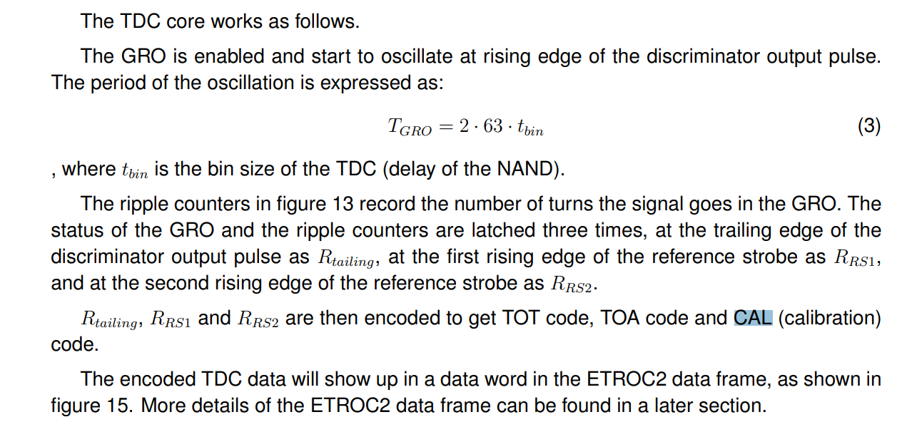
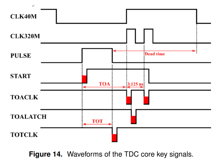
> Explain how clock picture makes sense
## Data Format of ETROC
A data payload of the ETROC has a header, data word, and trailer. The header and trailer are just predefined bits that tell you if it is the start or end of data (the I2C start and stop conditions!).
So this is a data word of the ETROC

Each of the codes can be converted to physical times or values by equations given in the ETROC manual
## Noise and Uncertainty in Time from ETROC / LGAD
## I2C Communication Protocol Notes
In this section I will go over what the I2C communication protocol is and where it is relevant in the Test Stand. Understanding I2C is not a bad idea for the system but recognizing the lingo that is relevant to it is important!
I2C is a communication protocol and uses the Serial Data Line and the Serial Clock Line. Communication is sent in byte packets with a unique address for each target device. Now I2C has a lot of terminollogy for some reason so there is a vocab section.
Example of I2C connection:
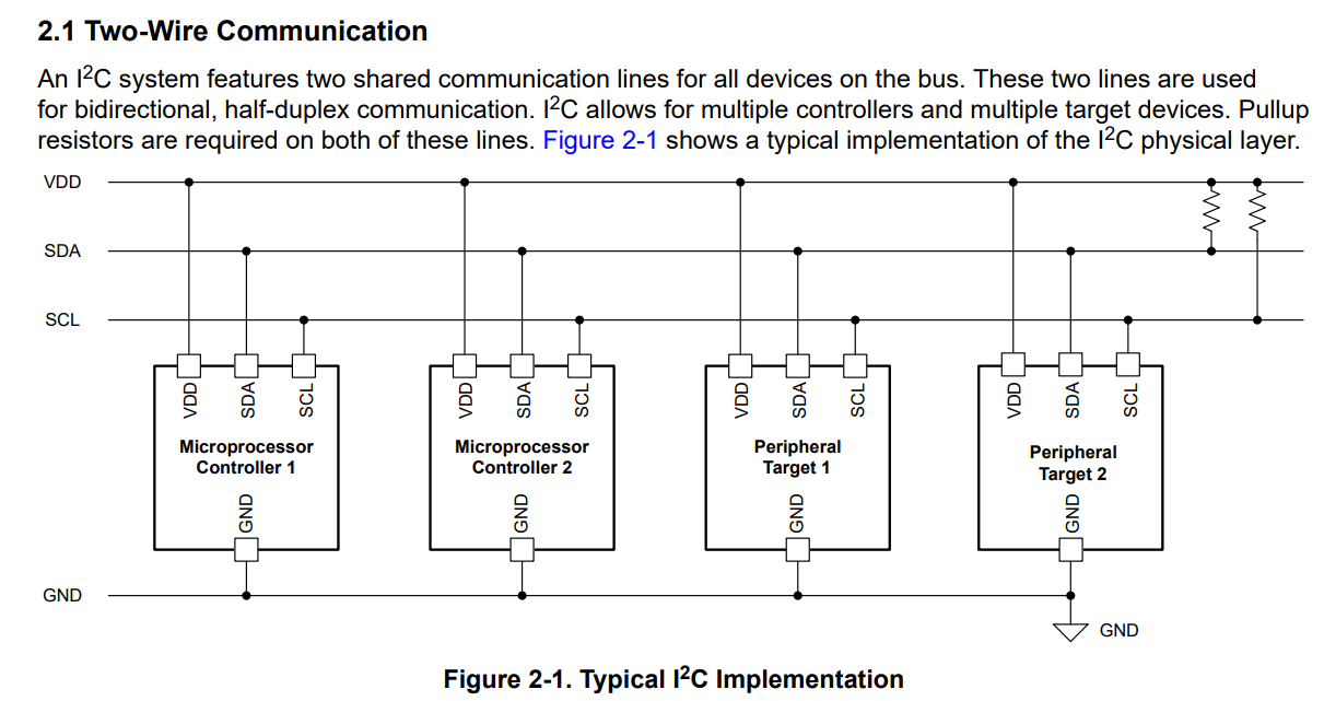
Analogous to our setup:
> INSERT PHOTO OF OUR SETUP IN THIS PICTURE, DESCRIBE HOW EACH WOULD CLAIM THE BUS WITH A START CONDITION OR ONE WOULD TALK TO THE OTHER!
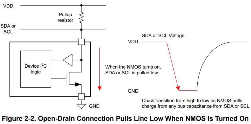
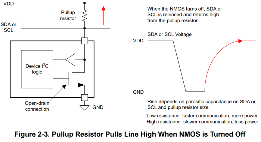
### How the lines are set high (1) or low (0) by the lpGBT (or any device that does I2C)
In chapter 2.2 it explains this https://www.ti.com/lit/an/sbaa565/sbaa565.pdf but I will try to give more understanding to make it clear.
The pull up resistors connect both the SCL and SDA line to the power. There is an important conceptual understanding to pull up resistors,it is *assumed* that the critical components have **infinite or sufficiently high impedance**, which is guaranteed for example for logic gates made from FETs.
* When the **switch is open**, the voltage across a pull-up resistor (with sufficiently low impedance) practically vanishes, and the circuit looks like a wire connected to VCC.
* LOGIC LEVEL = 1
* NMOS is turned **OFF** preventing current and keeping the voltage high (because of assumption for pull up resistor)
* When the **switch is closed**, the pull-up resistor must have sufficiently high impedance in comparison to the closed switch to not affect the connection to ground.
* LOGIC LEVEL = 0
* NMOS is turned **ON** allowing current flow and the full voltage to drop across the line
(This info can be used to [calculate pull up resistor](https://www.ti.com/lit/an/slva689/slva689.pdf?ts=1721147318139&ref_url=https%253A%252F%252Fwww.google.com%252F#:~:text=The%20pullup%20resistors%20pull%20the,by%20the%20open%2Ddrain%20interface.) values in I2C)
The left diagram is essentially the same as the third (switch open). Remember a transistor (NMOS) works just like a switch (High V on transistor opens drain, low V on transistor closes drain).
| Pull Up Resistor | Pulling Low (NMOS ON) | Pulling High (NMOS 0FF) |
| -------- | -------- | -------- |
|  |  |  |
### How 1s and 0s are read from I2C and data sent
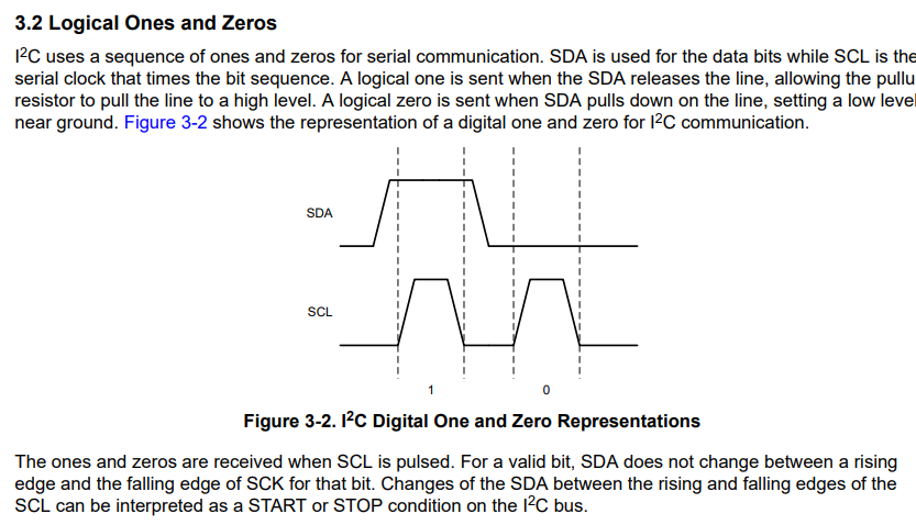
So data can be sent like this:

The format is [START]-[ADDRESS]-[ACKNOWLEDGE BIT]-[DATA]-[ACKNOWLEDGE BIT]-[STOP]
### Important things to remember
* Every device on the I2C bus has an address, the slave lpGBT, the ETROCs etc... all have an address used by the I2C bus
* For example, a temperature sensor could have address of 0x40. What does the “0x” mean in this address? It means that the number that follows is in hexadecimal notation, base 16 instead of base 10
### Vocab
* **SDA**: Serial Data Line one of the two lines for I2C
* **SCL**: Serial Clock Line one of the two lines for I2C
* **"Pulling low or high"**: low or high means ground or Vcc/Vdd respectively, which correspond to a logical 1 or 0!
* **Bus**: like a physical bus, the bus is a mode of transporting data between two location. We are learning about the I2C bus
* **open-drain**: means the device can pull a level down to ground, but cannot pull the line up to Vdd. Hence the name open-drain
* **Vcc**: https://en.wikipedia.org/wiki/IC_power-supply_pin
* **Pull Up Resistors**: https://en.wikipedia.org/wiki/Pull-up_resistor
### Resources
* SDA in software? https://gitlab.cern.ch/cms-etl-electronics/module_test_sw/-/blob/master/tamalero/SCA.py
* Pull Up Resistor Calculation https://www.ti.com/lit/an/slva689/slva689.pdf?ts=1721067502788
* What is Vcc? ts=1721065730507&ref_url=https%253A%252F%252Fwww.google.com%252F#:~:text=The%20first%20line%20is%20SCL,to%20or%20from%20target%20devices
* https://www.ti.com/lit/an/sbaa565/sbaa565.pdf?
* I2C for dummies https://www.dummies.com/article/technology/programming-web-design/python/what-is-i2c-python-programming-basics-for-the-raspberry-pi-264864/
* Wiki: https://en.wikipedia.org/wiki/I%C2%B2C
## What is an ADC?
## How does a Clock work?
Typically a clock tells you when to read data.
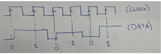
You can see by comparing the clock to the data pulse how we get our 1s and 0s for our data!
## Voltage
Voltage refresher (yikes!),
If the electric potential difference between two locations is 1 volt, then one Coulomb of charge will gain 1 joule of potential energy when moved between those two locations.
All you need is a difference in charge between two points. This sets up an electric field. The energy per unit charge to move a charge is the voltage.
Also voltage doesn't actually “travel" through a wire. It is more like a difference of potential existing across the ends of a wire or circuit.
## Addresses, Registers, Machine Code and CPUs
(idea is this is a common thing I know, which could help relate to test stand software to FPGA?)
If you ask most people what is a CPU, what does it do? They would say ah its the central processing unit, the brains of computer, or that is where the calculations take place. But what heck exactly is a CPU and how do we interface with it?
### CPU
A CPU is a piece of hardware that runs instructions (program code, operating system code, reads and writes to memory, and does computations). These instructions are very basic things, lets for example take the [MOS6502](https://en.wikipedia.org/wiki/MOS_Technology_6502) which was a very popular processor (it was in the Atari, nintendo, apple 2 computers). It cannot multiply or divide, sine or cosine, or a lot of things a basic calculator could do. It implements just enough instructions to make anything else doable in software (roughly the definition of a turing machine). The MOS6502 implemented add, subtract, compare, jump, jump subroutine, and return subroutine (but I won't get into exactly what all those are).
Processors do not have variables they have **registers**, these are literal pieces of hardware that register some value that are used as temperory areas for work by the CPU. With a CPU you do not get to do x+y, you have to move x into a register and then it tell it to add with y, then the result will be in that register. So then you have to copy it out and put it where you want it.
### Machine Code
There is a really nice conceptualization of how addressing, accumulators, etc... work for machine code: https://www.youtube.com/watch?v=8VsiYWW9r48
* See second [stack overflow answer](https://electronics.stackexchange.com/questions/476334/where-are-registers-and-what-do-they-look-like), transistor to NAND gate, to flip flop, to **latch**, to register.
* [latches and flip flops](https://www.cs.ucr.edu/~ehwang/courses/cs120b/flipflops.pdf)
# Notes
CERN Power Supply IP address: 192.168.0.25 and [manual](https://siglentna.com/wp-content/uploads/dlm_uploads/2023/04/SPD3000X-Series-Service-Manual_E01B.pdf)
# Daniel Info Notes
Address Tables
Address tables for firmware of KCU - downloaded the latest version - for every command to KCU you specify register you right 1 to and the register needs a physical address.
Each part has an address table, you can see in the manual.
Configuration files has the addresses for the lpGBT I2C communication, so I2C needs address.
Slow Control - you go through I2C it is not fast, you run once or every couple seconds. It is how we communicate with the ETROC.
Fast Control -
If you want a method to add with the etroc you do read and write registers.
modulev1_v2 (module v1 for etroc v2)
Elinks tries to find
When you send a high logic level one in software:
- you write a configuration into some register on the KCU, the KCU sends a command through the optical links to the lpGBT and the lpGBT does whatever it is told to do, writes to I2C bus, or sets GPIO high or low
register